Ceramic film by Aerosol Deposition Process (AD Film)
TOTO developed a unique Y2 O3 film application by aerosol deposition (AD) process that provides outstanding plasma resistance for applications in semiconductor production equipment. By applying a fine layer of Y2 O3 film to various substrates, including metals, quarts and ceramics, TOTO's unique AD film enhances plasma corrosion resistance and contributes to reductions in particle contamination.
What is AD Film?
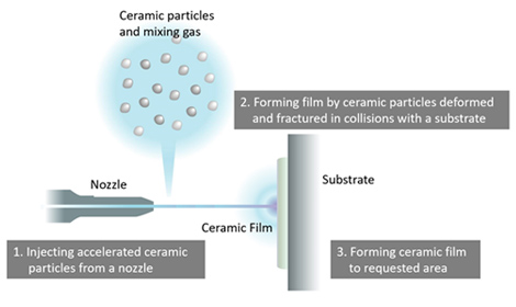
AD process uses an aerosol by mixing submicron level ceramic powders and carrier gas at room temperature that will be accelerated through the nozzle and crashed onto the substrate at a sonic velocity of 150-400 m/s.
The crash deposits highly dense ceramic film with excellent adhesion thanks to the compound dense nano crystallites and the anchor layer against the substrate. [Figure 1]
This technology overturns the common sense of ceramics need to be sintered and is expected to satisfy various market needs.
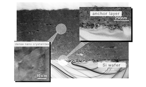
[Figure 1] Structure of ceramic film by AD process
*Cross-Sectional TEM Micrograph.
AD Film Materials
AD film is available with different ceramic materials, such as Y2 O3 , which has excellent plasma resistance, Al2O3 , BaTiO3 and other oxide or compound oxide material. TOTO expands AD film to different applications in multiple markets by choosing optimized material for each application.
Charasteristic of Y2 O3 Film
Due to its high plasma resistance, Y2 O3 film by AD process has been used as a coating to parts inside the chamber of semiconductor production equipment. AD process enables to fabricate highly dense Y2 O3 film without voids whereas conventional methods such as thermal spray and sintered bulk have a lot of voids. [Figure 2] AD film shows the best performance towards plasma exposure test in terms of surface roughness change. [Figure 3] This means that the particles in semiconductor production equipment from AD film are extraordinary less than conventional methods that contribute to improvements in the yield of the semiconductor manufacturing process.
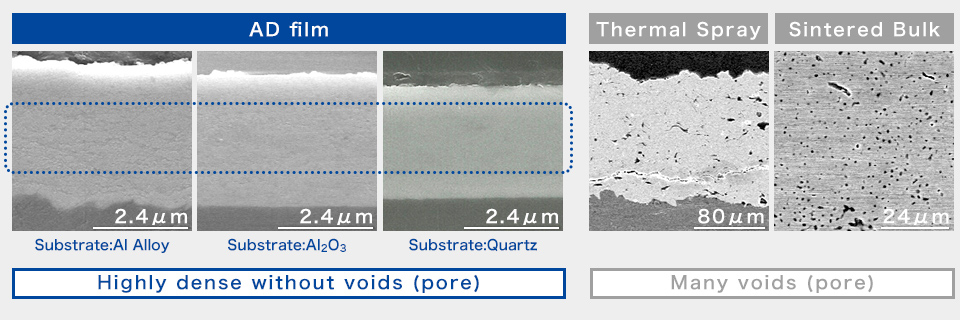
[Figure 2]Y2O3 Comparison between AD film and conventional method.
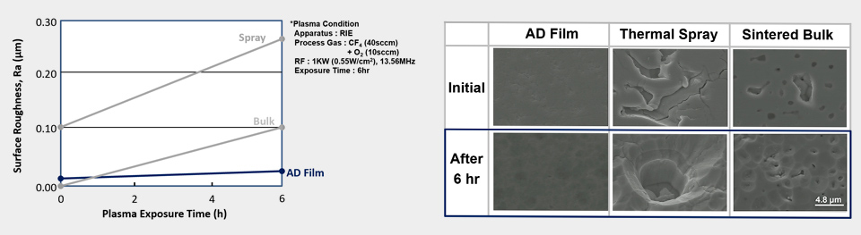
[Figure 3] Plasma Exposure Test *Plasma exposed for 6 hours under the same conditions.